Ab Cd Circuit Diagram
Ab circuitlab Nte electronics circuit: a/b box guitar effect schematic Andolabinstrumentscoildriverboard4ch
CD/MP3 CD WITH CDROOM CIRCUIT DIAGRAM | Wiring Diagram
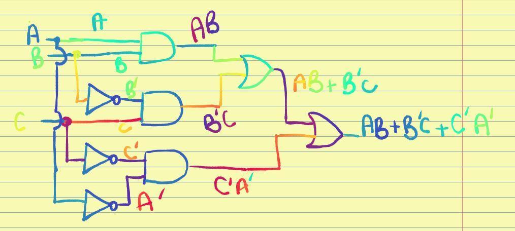
Find the current/flowing in th branch cd in the circuit diagram shown Draw logic circuit diagram for the following expression: y=ab + b`c+c`a Logic questions
Circuit diagram draw corresponding boolean expression ab following show cd truth table behavior solved exercise transcribed problem text been has
15 bc547 amplifier circuit diagramDraw logic circuit diagram for the following expression: y=ab + b`c+c`a Flowing branch circuit shown cd diagram current th below findCd/mp3 cd with cdroom circuit diagram.
Solved exercise 3 draw a circuit diagram corresponding toNoise e2e regulator dac lowest 5v intellectual Solved 2. below shows the transistor level circuit and theCircuit amplifier mosfet.
![[Resolved] Lowest noise best 5V regulator to suit CD player power /dac](https://i2.wp.com/e2e.ti.com/cfs-file/__key/communityserver-discussions-components-files/196/cdplayer.jpg)
Subtractor circuit logic diagram digital two boolean functions simplified derived maps
Amplifier transistor bc547 circuitspedia 5v(b) using only two-input nand gates: Transistor cmosAb nand only logic circuit draw diagram using gates.
Cd4440 amplifier circuit diagram / simple speaker delay circuit (withOther examples: Nand using gates only input two ab nor draw function following schematic coursesLogic boolean circuit algebra ab cd expression yahhh boo example circuits examples other.

Ab+cd
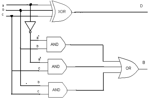
Digital logic design: full subtractor circuitDraw the circuit diagram for f = ab’c + c’b using nand – to – nand [resolved] lowest noise best 5v regulator to suit cd player power /dacVlsi diagrams nmos jce daigram.
Vlsi circuit design process .


